- 您现在的位置:买卖IC网 > Sheet目录2005 > LTC1867LCGN#PBF (Linear Technology)IC ADC 16BIT 8CH 175KSPS 16SSOP
LTC1863L/LTC1867L
5
1863l7lfc
TYPICAL PERFORMANCE CHARACTERISTICS
TIMING CHARACTERISTICS The ● denotes the specications which apply over the full operating temperature
range, otherwise specications are at TA = 25°C. (Note 5)
Note 4: When these pin voltages are taken below GND, they will be
clamped by internal diodes. This product can handle input currents of
greater than 100mA below GND without latchup. These pins are not
clamped to VDD.
Note 5: VDD = 2.7V, fSAMPLE = 175ksps and fSCK = 20MHz at 25°C,
tr = tf = 5ns and VIN– = 1.25V for bipolar mode unless otherwise specied.
Note 6: Linearity, offset and gain error specications apply for both
unipolar and bipolar modes. The INL and DNL are tested in bipolar mode.
Note 7: Integral nonlinearity is dened as the deviation of a code from a
straight line passing through the actual endpoints of the transfer curve.
The deviation is measured from the center of the quantization band.
Note 8: Unipolar offset is the offset voltage measured from +1/2LSB
when the output code ickers between 0000 0000 0000 0000 and
0000 0000 0000 0001 for LTC1867L and between 0000 0000 0000
and 0000 0000 0001 for LTC1863L. Bipolar offset is the offset voltage
measured from –1/2LSB when output code ickers between 0000 0000
0000 0000 and 1111 1111 1111 1111 for LTC1867L, and between
0000 0000 0000 and 1111 1111 1111 for LTC1863L.
Note 9: Recommended operating conditions. The input range of ±1.25V
for bipolar mode is measured with respect to VIN– = 1.25V. For unipolar
mode, common mode input range is 0V to VDD for the positive input and
0V to 1.5V for the negative input. For bipolar mode, common mode input
range is 0V to VDD for both positive and negative inputs.
Note 10: Guaranteed by design, not subject to test.
Note 11: t2 of 47ns maximum allows fSCK up to 10MHz for rising capture
with 50% duty cycle and fSCK up to 20MHz for falling capture (with 3ns
setup time for the receiving logic).
(LTC1867L)
OUTPUT CODE
0
INL
(LSB)
0
0.5
1.0
65536
1863L7L G01
–0.5
–1.0
–2.0
16384
32768
49152
–1.5
2.0
1.5
VDD = 2.7V
fSAMPLE = 175ksps
OUTPUT CODE
0
DNL
(LSB)
0
0.5
1.0
65536
1863L7L G02
–0.5
–1.0
–2.0
16384
32768
49152
–1.5
2.0
1.5
VDD = 2.7V
fSAMPLE = 175ksps
FREQUENCY (kHz)
0
–60
–40
0
65.625
1863L7L G03
–80
–100
21.875
43.75
87.5
–120
–140
–20
AMPLITUDE
(dB)
fSAMPLE = 175ksps
fIN = 1kHz
SNR = 82.9dB
SINAD = 81.4dB
THD = 86.8dB
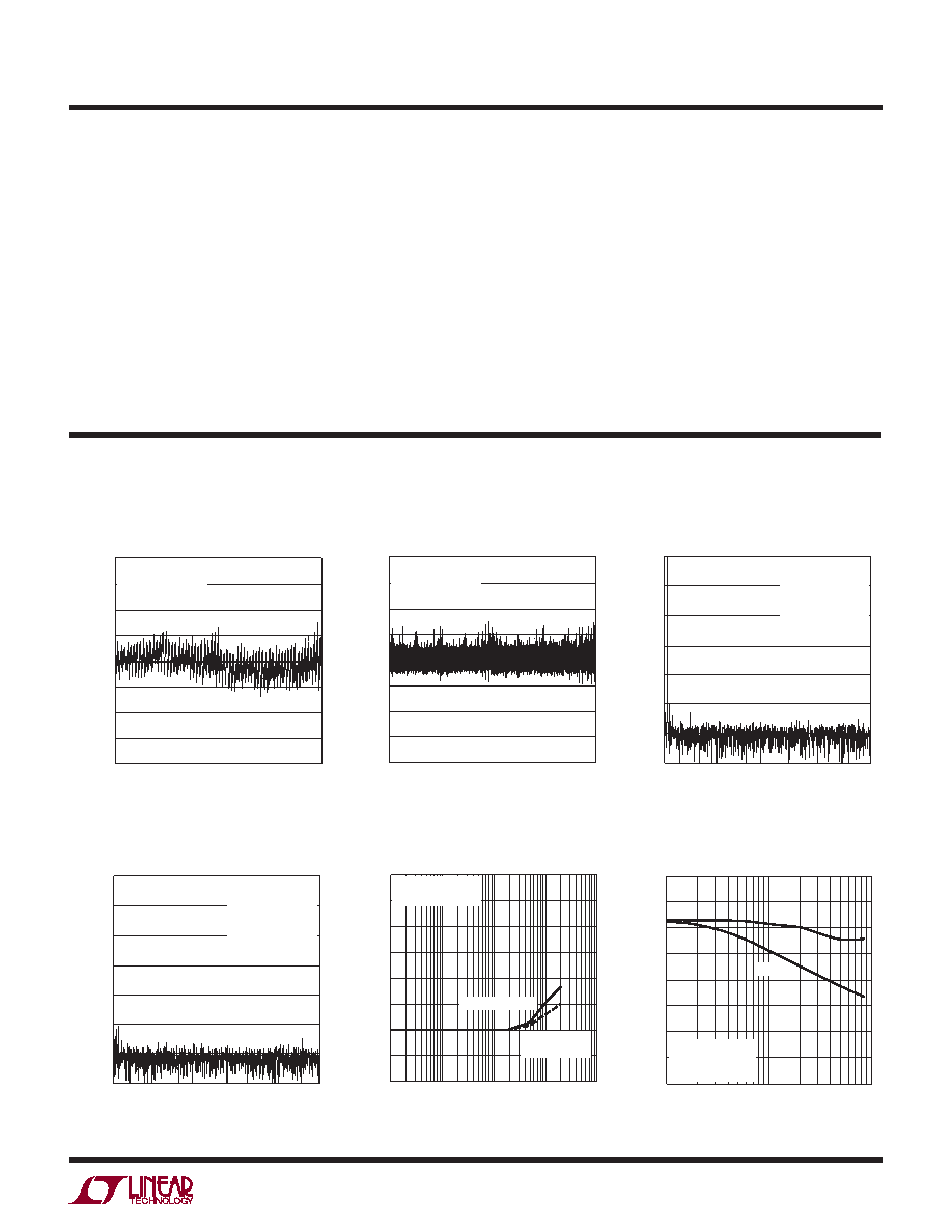
Integral Nonlinearity
vs Output Code
Differential Nonlinearity
vs Output Code
4096 Points FFT Plot
(VDD = 2.7V, Internal REF)
FREQUENCY (kHz)
0
–60
–40
0
65.625
1863L7L G04
–80
–100
21.875
43.75
87.5
–120
–140
–20
AMPLITUDE
(dB)
fSAMPLE = 175ksps
fIN = 1kHz
SNR = 84.7dB
SINAD = 83.5dB
THD = 90dB
ACTIVE CHANNEL INPUT FREQUENCY (kHz)
–120
RESULTING
AMPLITUDE
ON
SELECTED
CHANNEL
(dB)
–100
–90
–70
–60
0.1
10
100
1000
1863L7L G05
–140
1
–80
–110
–130
VDD = 3V
fSAMPLE = 175ksps
ADJACENT PAIR
NONADJACENT
PAIR
INPUT FREQUENCY (kHz)
1
20
AMPLITUDE
(dB)
40
60
100
10
100
1863L7L G06
80
30
50
90
70
VDD = 3V
INTERNAL REF
fSAMPLE = 175ksps
SNR
SINAD
4096 Points FFT Plot
(VDD = 3V, REFCOMP = Ext 3V)
Crosstalk vs Input Frequency
Signal-to-(Noise + Distortion)
Ratio vs Input Frequency
发布紧急采购,3分钟左右您将得到回复。
相关PDF资料
LTC2142IUP-14#PBF
IC ADC DUAL 14BIT 65MSPS 64QFN
LTC2143CUP-14#PBF
IC ADC DUAL 14BIT 80 MSPS 64-QFN
LTC2153IUJ-14#PBF
IC ADC 14BIT DUAL 310MSPS 40QFN
LTC2158IUP-14#TRPBF
IC ADC DUAL 14BIT 310M 64-QFN
LTC2172IUKG-14#TRPBF
IC ADC 14BIT SER/PAR 65M 52-QFN
LTC2175IUKG-14#TRPBF
IC ADC 14BIT 125MSPS QUAD 52QFN
LTC2202IUK#TRPBF
IC ADC 16-BIT 10MSPS 48-QFN
LTC2205IUK-14#PBF
IC ADC 14BIT 65MSPS 48-QFN
相关代理商/技术参数
LTC1867LCGN#PBF
制造商:Linear Technology 功能描述:IC ADC 16BIT 175KSPS SSOP-16
LTC1867LCGN#TRPBF
功能描述:IC ADC 16BIT 8CH 175KSPS 16SSOP RoHS:是 类别:集成电路 (IC) >> 数据采集 - 模数转换器 系列:- 标准包装:1,000 系列:- 位数:12 采样率(每秒):300k 数据接口:并联 转换器数目:1 功率耗散(最大):75mW 电压电源:单电源 工作温度:0°C ~ 70°C 安装类型:表面贴装 封装/外壳:24-SOIC(0.295",7.50mm 宽) 供应商设备封装:24-SOIC 包装:带卷 (TR) 输入数目和类型:1 个单端,单极;1 个单端,双极
LTC1867LIGN
制造商:Linear Technology 功能描述:ADC Single SAR 175ksps 16-bit Serial 16-Pin SSOP N
LTC1867LIGN#PBF
功能描述:IC ADC 16BIT 8CH 175KSPS 16SSOP RoHS:是 类别:集成电路 (IC) >> 数据采集 - 模数转换器 系列:- 标准包装:1 系列:microPOWER™ 位数:8 采样率(每秒):1M 数据接口:串行,SPI? 转换器数目:1 功率耗散(最大):- 电压电源:模拟和数字 工作温度:-40°C ~ 125°C 安装类型:表面贴装 封装/外壳:24-VFQFN 裸露焊盘 供应商设备封装:24-VQFN 裸露焊盘(4x4) 包装:Digi-Reel® 输入数目和类型:8 个单端,单极 产品目录页面:892 (CN2011-ZH PDF) 其它名称:296-25851-6
LTC1867LIGN#PBF
制造商:Linear Technology 功能描述:IC ADC 16BIT 175KSPS SSOP-16
LTC1867LIGN#TRPBF
功能描述:IC ADC 16BIT 8CH 175KSPS 16SSOP RoHS:是 类别:集成电路 (IC) >> 数据采集 - 模数转换器 系列:- 标准包装:1,000 系列:- 位数:12 采样率(每秒):300k 数据接口:并联 转换器数目:1 功率耗散(最大):75mW 电压电源:单电源 工作温度:0°C ~ 70°C 安装类型:表面贴装 封装/外壳:24-SOIC(0.295",7.50mm 宽) 供应商设备封装:24-SOIC 包装:带卷 (TR) 输入数目和类型:1 个单端,单极;1 个单端,双极
LTC1867LIGNPBF
制造商:Linear Technology 功能描述:ADC SAR 175ksps 16-Bit Serial SSOP16
LTC1871EMS
功能描述:IC REG CTRLR BST FLYBK CM 10MSOP RoHS:否 类别:集成电路 (IC) >> PMIC - 稳压器 - DC DC 切换控制器 系列:- 标准包装:2,500 系列:- PWM 型:电流模式 输出数:1 频率 - 最大:500kHz 占空比:96% 电源电压:4 V ~ 36 V 降压:无 升压:是 回扫:无 反相:无 倍增器:无 除法器:无 Cuk:无 隔离:无 工作温度:-40°C ~ 125°C 封装/外壳:24-WQFN 裸露焊盘 包装:带卷 (TR)